- Qualcomm Launches Snapdragon 4 Gen 2 Mobile Platform
- AMD Launches Ryzen PRO 7000 Series Mobile & Desktop Platform
- Intel Launches Sleek Single-Slot Arc Pro A60 Workstation Graphics Card
- NVIDIA Announces Latest Ada Lovelace Additions: GeForce RTX 4060 Ti & RTX 4060
- Maxon Redshift With AMD Radeon GPU Rendering Support Now Available
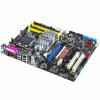
ASUS P5N-E SLI

When the 680i chipset was launched last month, it proved to have exactly what the enthusiast was after. However, most of those boards range in the $250 area. ASUS has just released their new P5N-E SLI board which offers the 650i chipset. It’s a scaled down version of it’s bigger brother, but costs far less and still contains a huge punch for enthusiasts.
Page 4 – Inside the BIOS
Since this is a budget board, I was curious as to how much functionality and flexibility the BIOS offered. Would this prove to be an ultimate budget overclockers board?
ASUS chose to use a Pheonix AwardBIOS here, which should feel right at home for many. The first screen you will see delivers all of the options regarding the date, time and hard drive configuration. By default, is enabled and HDD SMART is disabled. This seems strange to me, as it would normally make sense for those two options to be switched around. If you want SMART capabilities from the get go, make sure to enable it here.
The Advanced tab is where all of the overclocking action happens. You will need to switch the AI Tuning to Manual to have full control, or you can choose automatic overclocking if you don’t feel like stepping into the time consuming world of tweaking.
Under the System Clocks submenu is a single option… PCI-Express frequency. Voltage Control is where some fun begins, however. By default, all of these are set to Auto, which should be perfectly suitable for stock speeds. VCore allows a full range of flexibility, from 0.83125v all the way up to 1.6v in increments of 0.00625v.
The full vdimm range is as follows: 1.920v, 2.013v, 2.085v, 2.178v, 2.259v, 2.353v, 2.424v and 2.517v. This may seem low compared to some other enthusiast boards, but more often than not, you don’t need more voltage for a bigger overclock. I’ve often seen overclocks of DDR2-1200 using only 2.2v. If you have good memory chips, you shouldn’t need a huge amount of vdimm.
The last Voltage option here is for your northbridge, and its options are: 1.208v, 1.393v, 1.563v and 1.748v.
The FSB & Memory Config portion of the BIOS proved to be the one I was inside of most frequent. This section also proves that just because of it’s budget moniker, it’s not about to hold you back from an insane overclock.
The first option in the menu allows you to either Link or Unlink the FSB and Memory. This is as to say, will your CPU/Mem scale to each other using the usual dividers, or not? If you choose Linked, you will have an option of a 1:1, 5:4 or 3:2 divider. If you are running PC2-8500 memory and plan to run your C2D at stock speed, you would run a 1:1 divider to make both the FSB and DDR2 speed 1066MHz.
Unlinked is the option I chose to use though, because thanks to NVIDIAs memory controller, there is a lot more flexibility here. As an example, at one time I chose to use a 375FSB (1500MHz) and then 800MHz for the ram, or DDR2-800. This gave me a divider of 15:16. As odd as it is, it works and works well. This essentially means that your ram should not be the factor for your CPU overclock not being able to reach new heights. I am unsure how out of whack the dividers go, but it certainly didn’t stop me from reaching my max CPU overclock.
|
|
Support our efforts! With ad revenue at an all-time low for written websites, we're relying more than ever on reader support to help us continue putting so much effort into this type of content. You can support us by becoming a Patron, or by using our Amazon shopping affiliate links listed through our articles. Thanks for your support!


