- Qualcomm Launches Snapdragon 4 Gen 2 Mobile Platform
- AMD Launches Ryzen PRO 7000 Series Mobile & Desktop Platform
- Intel Launches Sleek Single-Slot Arc Pro A60 Workstation Graphics Card
- NVIDIA Announces Latest Ada Lovelace Additions: GeForce RTX 4060 Ti & RTX 4060
- Maxon Redshift With AMD Radeon GPU Rendering Support Now Available
Social & RSS Feeds
Latest Videos

Latest News
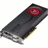
AMD Radeon HD 6950 & HD 6970 2GB
by Rob Williams on December 20, 2010 in Graphics & Displays
Not wanting to end 2010 without the last word, AMD unveiled its Radeon HD 6900 cards last week. These cards bring a couple of interesting features, including a revamped architecture, improved power handling, dual BIOS support, EQAA anti-aliasing and more. With NVIDIA’s GTX 570 just launched, let’s see where AMD stands with its new cards.
Page 2 – Closer Look at AMD’s HD 6900 Series
As mentioned at the outset, AMD has built its Radeon HD 6900 GPUs on a 40nm process, which is the same one used for the entire HD 5000 series and also the mid-range HD 4770 card. As nice as it would have been for AMD to deliver 32nm releases here, it decided to not mope around the idea and instead pursued ways to improve the architecture further, and also amp up performance where possible.
To sum up the HD 6900 series from a technical standpoint, AMD classifies it by saying, “The time for high performance DirectX 11 is now!”, and it can say this as the performance with DirectX 11 in particular has increased quite a bit since its Cypress launch. As a result, tessellation performance sees a nice increase, although NVIDIA remains ahead in overall performance.
With the HD 6900, AMD’s design goals were to create a more efficient product, one that has massive geometry performance, improved image quality features and of course, is more power efficient. It accomplishes all this a couple of different ways.
First, a VLIW4 arrangement has been implemented. What’s that stand for, and what’s it mean? It stands for “Very Long Instruction Word” (thanks Charlie), and it refers to the overall organization of the components in the GPU. In gist, VLIW4 is more efficient than VLIW5, and was a necessary change thanks to the fact that AMD was working with a similar die size, but still trying to fit in more performance and features.
Here’s a pretty die diagram that we’ve all come to expect from AMD:

Moving to a VLIW4 configuration to VLIW5 in itself doesn’t automatically deliver a performance increase, but it has allowed AMD to make more efficient use of the space it’s given.
In addition to this change, back-end render engines have also been improved, with up to 4x performance in some calculation processes, and not surprisingly, GPU compute performance has also been tackled. AMD has introduced asynchronous dispatch to allow each computer kernel its own command queue in a protected virtual address domain, which is in essence improved threading, and should prove quite beneficial overall.
One of the bigger changes is the move to dual graphics engines, allowing two primitives to be processed per clock, which is one of the bigger reasons tessellation performance has been improved, by up to ~3x. You can see this exampled in this slide:

You might notice that instead of comparing the HD 6970 to the GTX 480 or 580 for tessellation performance, AMD has compared it to the HD 5870 instead. This could be considered proof that NVIDIA’s tessellation performance is still quite a bit ahead, as it should be given the amount of development time NVIDIA has sunk into Fermi’s computational performance.
With the HD 6800 series, AMD introduced a new anti-aliasing mode called Morphological AA, which differed from typical AA modes in that it acts as a post-processor. With the HD 6900 series, the company has once again improved on its anti-aliasing options by offering “EQAA”, a mode that doubles the number of coverage samples from MSAA, as seen here:

We haven’t had the chance to delve deeper into the real improvements to be gained with EQAA, but it’s something we’d like to tackle soon, in addition to Morphological AA, as we haven’t dealt too deeply with that up to this point either.
What might be the most significant change to the architecture of the HD 6900 series is the introduction of “PowerTune”, a power-related technology that assures the GPU in question doesn’t exceed its set max wattage (TDP) value. In the case of the HD 6970, which features a TDP of 250W, PowerTune would keep that value in check during use, and not exceed it which is becoming so common of GPUs today.

PowerTune works by employing an integrated control processor to monitor the current (no pun) power draw of the card, and when things are getting a bit too heated, it will decrease the clocks in order to keep the TDP from going over. Due to an efficient design, AMD states that this throttling shouldn’t result in a real noticeable performance drop, and in our tests, that’s not something we exhibited.
Because overclockers tend to push TDP levels far past recommended values, AMD includes a feature in its OverDrive utility that will allow you to either decrease the max TDP by 20%, or increase it by 20%. Why would you ever lower it? For HTPC use, and things like that, when you want things to be as low power as possible.
This tech is similar to the introduced by NVIDIA with the GeForce GTX 580. It’s good in theory, but makes it more difficult for reviewers to acquire “top” wattage draw values. Programs like OCCT and Furmark are rendered useless, so we’re in the process of replacing our power-stress test with something that should still deliver good results. We’re evaluating 3DMark 11, as it makes heavy use of multiple things that pushes a GPU hard.
We’ve been seeing “Dual BIOSes” on select motherboards for some times, because for overclockers, they act as a great failsafe. But, overclockers tackle GPUs also, so what’s the deal with the lack of a dual BIOS there? Well, there isn’t a lack, any longer. Note a brand-new switch:

The mechanics of this are simple. For normal use, the BIOS can be in the default position, and for flashing or insane overclocks, the secondary BIOS can be used. If something goes awry, you can simply switch to the safe BIOS in order to fix the second.
There are other minor additions to the HD 6900 series, but for the sake of time I can’t tackle them all. The last notable thing I’ll mention is that this series introduces the 5th generation “vapor chamber” GPU cooler design, although it’s not clear what changes have been made. The cooler is rather large as a result of the card being large, however, so overall, we should be able to expect some decent performance there.
We’ll talk a bit about our testing system and methodologies on the following page, and then will get to a look at the performance.

Support our efforts! With ad revenue at an all-time low for written websites, we're relying more than ever on reader support to help us continue putting so much effort into this type of content. You can support us by becoming a Patron, or by using our Amazon shopping affiliate links listed through our articles. Thanks for your support!

Rob Williams
Rob founded Techgage in 2005 to be an 'Advocate of the consumer', focusing on fair reviews and keeping people apprised of news in the tech world. Catering to both enthusiasts and businesses alike; from desktop gaming to professional workstations, and all the supporting software.


