- Qualcomm Launches Snapdragon 4 Gen 2 Mobile Platform
- AMD Launches Ryzen PRO 7000 Series Mobile & Desktop Platform
- Intel Launches Sleek Single-Slot Arc Pro A60 Workstation Graphics Card
- NVIDIA Announces Latest Ada Lovelace Additions: GeForce RTX 4060 Ti & RTX 4060
- Maxon Redshift With AMD Radeon GPU Rendering Support Now Available
Interview with Andy Keane of AGEIA

AGEIA is a company with huge ideas. They plan to make our gaming experiences much more immersive with their PhysX add-in card. We sit down and chat with Andy Keane to answer some burning questions.
Page 1 – Introduction
Back in May, around E3 time, AGEIA was responsible for a lot of buzz in the hardware industry. The world was talking about their promise to make our gaming experiences much more rich. This would come in the form of a Physics Processing Unit (PPU), called PhysX. For those who have not heard of AGEIA or PhysX before, I’ll delve a little into what you can expect to see more of in the future.
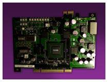
Basically, AGEIA (Stands for America, Germany, Egypt, India, America) created a PhysX PPU chip, which resides on a PCB board, which will be used in your PCI slot. The PhysX chip utilizes the NovodeX SDK. What the chip can do essentially, is handle mass amounts of physics operations.. much more than a normal CPU can. In fact, according to AGEIA, a current CPU can handle around 1,000 active bodies, while the PhysX chip can handle 32,000 with relative ease. With future software updates, that number could get even higher.
 Most of us who have played through games like Half-Life 2, realize how much good physics can add to the experience. If we rewind back to last year and had the AGEIA on hand then, we can imagine what the chip could have done to add to the experience even more.
There are a lot of skeptics out there though, and I for one, am one of them. What AGEIA promises to do, is quite extraordinary, and if they get the right support, which seems great so far, then this could be an add-in card that hardcore gamers cannot do without.
In gist, the PhysX card will allow for a much more rich gaming experience, due to the much larger physics capabilities. Hopefully down the road, more and more developers will pick up on this and make use of the NovodeX SDK. Currently, such companies as Shiny, Ritual, Cryptic, NC Soft and Epic have jumped on the bandwagon and plan to use the PhysX technology in their games. Even announced recently, the Sony Playstation 3 will be taking advantage of the NovodeX SDK as well.
What we know about the card specifications up to now is, that it will have 125,000,000 transistors, and a 182mm^2 die size. It uses a respectable 0.13µ process, and uses approx. 28 watts of power. Lastly, it will be equipped with 128MB or GDDR3 memory. In the picture to the right, you can see the overview of the card. You’ll notice that it’s dual sided for PCI-E and PCI. This will not be in the final card, but is only available in the developers version.
With all the information about the PhysX chip already, there were still some burning questions. We had the opportunity to chat with VP of Marketing, Andy Keane, to clear up these questions. I should also note, that all the images you see in the article can be clicked on for their original size.
Techgage: Greater physics capability sounds exciting, but since most gamers will likely be swayed away from the $249 – $299 price tag, do you have any specific plans to help really grab their attention, and gain an interest to buy?
Andy Keane: Content is king, and what will sell the hardware is the games. We’ve lined up a great deal of content, see enclosed presentation. Also, keep in mind, that consumer prices for graphics cards, and SLI are upwards of $400.
|
|
Support our efforts! With ad revenue at an all-time low for written websites, we're relying more than ever on reader support to help us continue putting so much effort into this type of content. You can support us by becoming a Patron, or by using our Amazon shopping affiliate links listed through our articles. Thanks for your support!


