- Qualcomm Launches Snapdragon 4 Gen 2 Mobile Platform
- AMD Launches Ryzen PRO 7000 Series Mobile & Desktop Platform
- Intel Launches Sleek Single-Slot Arc Pro A60 Workstation Graphics Card
- NVIDIA Announces Latest Ada Lovelace Additions: GeForce RTX 4060 Ti & RTX 4060
- Maxon Redshift With AMD Radeon GPU Rendering Support Now Available
Taking a Deep Look at NVIDIA’s Fermi Architecture
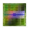
It has taken a bit longer than we all had hoped, but last week, NVIDIA gathered members of press together to dive deep into its upcoming Fermi architecture, where it divulged all the features that are set to give AMD a run for its money. In addition, the company also discussed PhysX, GPU Compute, developer relations and a lot more.
Page 1 – Introduction, GF100, Geometric Realism
During an editor’s day held by NVIDIA last week, the company delved deep into almost everything a gamer, or game developer, could care about. This includes of course discussion of the company’s upcoming GF100 graphics chip, based on the Fermi architecture, along with many updates on the state of PhysX, and even some talk on the development side of things, with APEX and Nexus.
This article will be split into a couple of different sections, with the first tackling what most of you will care most about, GF100. After we’re done exhausting what’s new there, we’ll continue onto a look at everything else NVIDIA discussed during this all-day event.
Before we get too far into the article, let’s make sure we’re all on the same line regarding what GF100, as the codename, is. There has been some confusion around GF100, given that for the previous generation of NVIDIA cards, both the codename and board names were equal to GT200. For the upcoming Fermi cards, that’s not exactly the case. The GF in GF100 stands for “Graphics Fermi”, and the actual card models themselves will likely follow previous schemes, eg: GTX 380.
The reason NVIDIA felt the need to “reset” the codename numbers, so to speak, is because Fermi is an entirely new architecture with a renewed set of goals, rather than a simple evolution of a previous architecture. I’m sure that as we’ll go further, future generations of Fermi will continue the naming scheme, eg: GF200, GF300, et cetera. But, NVIDIA stated that “GF100” isn’t entirely final, so it may possibly change before its launch.
When NVIDIA first unveiled Fermi this past fall, it became clear that the company saw a future in the typical graphics card being used for much more than simply generating graphics. Instead, the GPU looks to become an integral role for things like GPGPU (general purpose GPU) computing and also physics computation, PhysX and otherwise. As we saw with the initial Fermi information, we could see that NVIDIA was banking big on the architecture’s compute performance, and with as much R&D and money the company is pouring into things, we can hope the company’s focus is rightfully-set.
With GF100, NVIDIA had a couple of goals it set out to achieve. First, and most obvious, is that the GPU should be the highest performing to date, with even substantial gains over ATI’s current-gen HD 5000 series. Second, the geometric realism needs to be top-rate, and that also leads into the third goal, which is image quality. Finally, not only should Fermi excel for GPGPU, but also GPU compute for gaming, which can take many different forms, but most notably, physics.
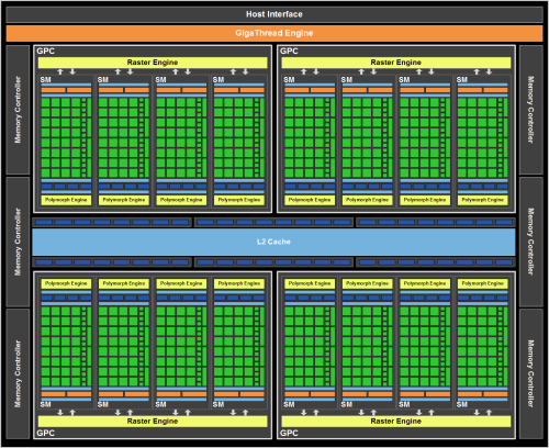
In the first meaty slide we were shown, we were re-introduced to Fermi’s block diagram, which was first shown at the company’s GTC conference last fall. Here, though, we were given a bit more information on things, including the specific number of components per chip, and also a first-look at a couple of new components, including the PolyMorph and Raster engine units. For the sake of easier explanation, I recommend looking at the full-view version of the diagram below:
- NVIDIA GF100 Architecture Specs
- 512 CUDA Cores
- 16 Geometry Units
- 4 Raster Units
- 64 Texture Units
- 48 ROP Units
- 768KB L2 Cache
- 384-bit GDDR5
- NVIDIA GF100 SM Specs
- 32 CUDA Cores (4x compared to GT200)
- 16 or 48KB of Shared Memory (3x compared to GT200)
- 16 or 48KB of L1 Cache (There was no L1 on GT200)
- ISA Improvements (32-bit int operations, IEEE-754 2008 FMA operation)
- 4 Texture Units
- 1 PolyMorph Engine
For the graphics processor that the above diagram represents, the chip is split up into four main clusters, or GPC’s (Graphics Processing Clusters), with each of these clusters split up into four SM’s (Streaming Multiprocessors), for a total of sixteen across the entire chip. All GF100 chips will follow this similar layout, but each model will of course be altered depending on its goals (a mid-range offering may only contain two GPC’s, for example).
Because the basic Fermi block diagram has been around for a while, I’m not going to focus on every aspect of the architecture, but rather focus on what was newly unveiled during the editor’s day. Most notably, these were the PolyMorph and Raster engines, both of which contribute to geometric realism. But what exactly is geometric realism, and why should so much of Fermi be focused on improving it?
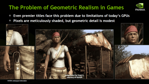
When NVIDIA began talking about geometric realism, it brought up what’s seen in film, where we never expect to see issues with things like lighting, shading, clipping and so forth. Rather, it’s perfect. But to accomplish something like this, you need major PC horsepower… there’s a reason these large movie studios run hundreds, if not thousands, of computers for the sole purpose of rendering. To emphasize the issue, consider the fact that for the typical PC game, the average polygons per frame is between one – two million. For a feature film? Hundreds of millions.
Needless to say, it’s not realistic to expect the same level of geometric realism in a PC game, regardless of how powerful our computers are. But here’s another interesting fact. While pixel shaders have had an increasing focus from GPU generation to the next, there’s been almost no love to the triangle generator. Compared to the GeForce FX (2003), the shading horsepower has increased by 150x, while the geometric processing has increased by only 3x. That about speaks for itself.
Support our efforts! With ad revenue at an all-time low for written websites, we're relying more than ever on reader support to help us continue putting so much effort into this type of content. You can support us by becoming a Patron, or by using our Amazon shopping affiliate links listed through our articles. Thanks for your support!


