- Qualcomm Launches Snapdragon 4 Gen 2 Mobile Platform
- AMD Launches Ryzen PRO 7000 Series Mobile & Desktop Platform
- Intel Launches Sleek Single-Slot Arc Pro A60 Workstation Graphics Card
- NVIDIA Announces Latest Ada Lovelace Additions: GeForce RTX 4060 Ti & RTX 4060
- Maxon Redshift With AMD Radeon GPU Rendering Support Now Available
JEDEC’s HBM Update: 12 Layer, 24GB Stack Of Memory
The global standards developer, JEDEC, responsible for the creation and updating of various microelectronics standards used in the tech industry, has announced the publication of its JESD235 High Bandwidth Memory DRAM standard. HBM is the high-performance alternative to GDDRX type memory used extensively by GPU manufacturers, and this latest update standardised the format for higher densities and bandwidth.
This isn’t about HBM3 or the like, but more of a manufacturing and integration update. Traditional memory like GDDR is typically installed as single-chip packages, laid out around the GPU. HBM allows for the stacking of multiple chips on top of each other, reducing PCB density. This latest JEDEC update now accounts for chips to be layered anywhere from two layers, four, eight, and up to 12, using a process called Through-Silicon Via (TSV), where the connections for the pins are etched through the chip, so that they can be stacked.
Using 16Gb-layer chips (gigabit), up to 24GB (gigabyte) of memory can be addressed from a single stack. The same 1024-bit interface is still in use, which can be divided up into 8 channels on a single stack. The per-pin bandwidth has had a moderating improvement to 2.4Gbps, allowing for a total memory bandwidth of 307GB/s, up from the previous JEDEC standard of 256GB/s.
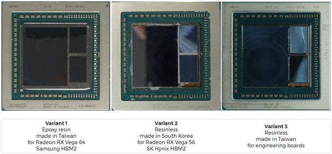
Some memory vendors like Samsung and SK Hynix, have already produced HBM2 memory that meets these speeds, however the JEDEC standard now offers those speeds for up to 12-layers. Increasing the number of layers is non-trivial while still maintaining the same speed.
When we will see the new stacking and speeds will be up to manufacturers and designers. Since AMD has been an avid user of HBM for a while now, we may see either higher memory density, or possible lower prices – although the standard makes no reference to pricing, as that is up to suppliers.


