- Qualcomm Launches Snapdragon 4 Gen 2 Mobile Platform
- AMD Launches Ryzen PRO 7000 Series Mobile & Desktop Platform
- Intel Launches Sleek Single-Slot Arc Pro A60 Workstation Graphics Card
- NVIDIA Announces Latest Ada Lovelace Additions: GeForce RTX 4060 Ti & RTX 4060
- Maxon Redshift With AMD Radeon GPU Rendering Support Now Available
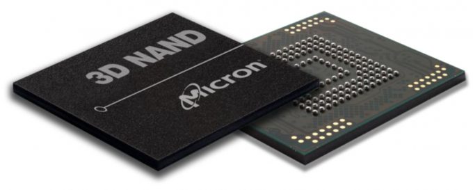
Micron Announces 2nd Gen 64-Layer 3D NAND Flash – Up To 256GB Chips
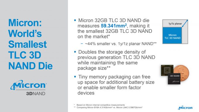
About 18-months ago, we were on call with Micron with its first generation 64-layer 3D NAND flash chips, which were quite impressive at the time. A lot can happen in those 18-months as Micron goes from 8GB in a 59mm2 pack, to 32GB, not just through process size reductions, but also through some clever stacking techniques.
For those that are not familiar, 3D NAND is where the flash storage cells are built up like a tower, using 3D transistors, rather than planer or flat transistors. This allows for better gate sizes and improved signal integrity while reducing the overall footprint of the transistor. This is not to be confused with processes such as Through-Silicon Vias (TSV) which stacks silicon wafers on top of each other. Combining TSV with 3D NAND means you can achieve very impressive storage densities.
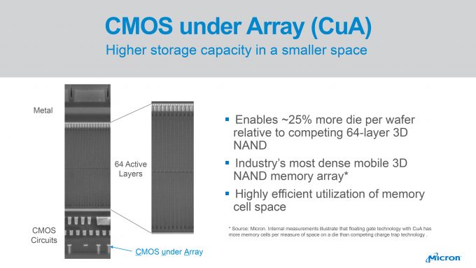
Regarding the 2nd generation 64-layer 3D NAND, Micron’s biggest achievement comes from its use of something called CMOS under Array (CuA), which places the power and logic array (what controls the signaling to and from the storage array) below the storage cells, rather than to the side. The picture below best shows this, as it’s a side-on view of the wafer (instead of top down). Micron described this setup as the basement to a tower-block.
This stacking and layers, complete with improved process shrinks means that Micron can manufacture 256GB single chip storage solutions for the mobile industry. Another important factor is speed, as these chips also make use of UFS 2.1, rather than e.MMC. UFS is not new, as Micron’s last 3D NAND chips also made use of the standard, but uptake of it has been fairly slow. More recently, UFS 2.1 has started to appear in flagship smartphones, but e.MMC is still the favorite for cheap storage. UFS is a serial, full-duplex (read and write at the same time) transfer standard, while e.MMC is a parallel half-duplex (read or write, not at the same time) standard.
One oddity of this launch is the mention of AI:
Micron’s mobile-optimized architecture utilizes an internal AI feature to monitor activity and temperature for the purpose of managing peak power and minimizing energy usage, achieving 2X power efficiency versus previous 3D NAND solutions.
This just seems like marketing running away with itself, using AI as another buzzword for a feature checklist, since previously, this would be simply labeled as power and temperature monitoring. Adding AI to the mix makes it sound so much more high-tech. Micron did bring up AI in other ways, as smartphones begin to make use of AI features that are not cloud-based. Having fast storage is important for these circumstances, such as with 4K video and large photos that need to be analyzed, and getting those assets out of storage and into memory quickly, is important.
In any case, high density storage is on the horizon, with capacities ranging from 32GB all the way up to 256GB, in single chip configurations with Micron’s 64-layer NAND TLC chips. With UFS 2.1 adoption becoming more prevalent as well, speed will become less of an issue as well. Micron still hasn’t fully outlined its 3D Crosspoint memory strategy at this point (similar to Intel’s Optane), but Flash storage will be around for quite some time.


