- Qualcomm Launches Snapdragon 4 Gen 2 Mobile Platform
- AMD Launches Ryzen PRO 7000 Series Mobile & Desktop Platform
- Intel Launches Sleek Single-Slot Arc Pro A60 Workstation Graphics Card
- NVIDIA Announces Latest Ada Lovelace Additions: GeForce RTX 4060 Ti & RTX 4060
- Maxon Redshift With AMD Radeon GPU Rendering Support Now Available
NVIDIA Teases Video On Its GPU Product Design Process
As part of its build-up to a new GPU launch, NVIDIA released today a short, documentary-style video on how it goes about product design, and the challenges that need to be overcome when building a new graphics card. While there is nothing particularly ground-breaking on show, the video does provide a high-level overview of thermal and electrical design – with a number of clear animations to boot.
We were not really sure what to expect when this video came through to our inbox, but at 8-minutes long, it was worth a look. It’s the usual high production value marketing strategy that we see, but there was some useful information buried in the video. For enthusiasts, there isn’t much on show, as it covers what we already know: GPUs use power, things get hot, cool stuff down, and make it look good in the process.
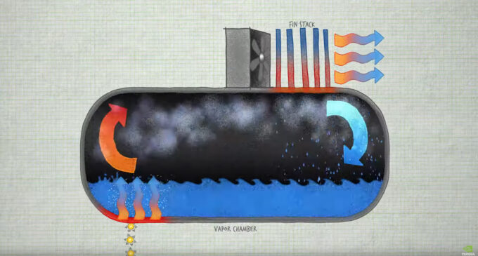
For those that don’t know about power density limits, vapor chambers, and just general product design, it’s worth a watch, especially with all the exploded diagrams of connected parts seamlessly melded together. It’s also nice to see some of the engineers working at NVIDIA doing some of the presentation.
Right at the beginning, we’re introduced to one of the fundamental problems behind modern electronics: power density. As we fit more components into a smaller space, and pump more power in to get those transistors switching, things get very hot, very quickly. NVIDIA noted that without a well-designed thermal solution, the temperature of the silicon die would reach temperatures of 760°C – or about 100°C above the melting point of aluminum.
A quick overview of thermodynamics and heat in a closed system ensues, and the role of a vapor chamber and cooling. We’re then presented with some of the mechanical elements, such as how a backplate is used to provide rigidity and support for the PCB and heatsink. The use of a new leaf spring instead of coiled springs to reduce the height of the mounting plate, provides more room for fins. There are mechanical stress tests to make sure the GPUs stand up to the literal drop-shipping that occurs by postal workers.
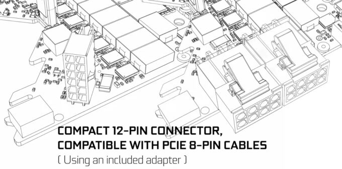
On the electrical side of things, we get a glimpse into some of the hidden challenges with high-density electronics, such as crosstalk. This is a process where signal lines running parallel leak into each other, causing interference and corruption. The way to get around this is through various tricks in layout and multi-layer PCBs. We’re also given our first official glimpse at the new 12-pin replacement connector for the dual 8-pin PCIe connectors that have been in use for quite a few years. This had been leaked previously from a couple of independent sources, but we get to see a much smaller connector that’s capable of delivering more power (plus an odd vertical attachment for the 12-pin, too). The remainder of the video covers some of the concept and visual designs of making a GPU.
NVIDIA will be holding a special event on September 1st as it builds up the hype for the new Ampere-based GeForce GPUs – 21 days and 21 years after NVIDIA’s first GPU, the GeForce 256.


