- Qualcomm Launches Snapdragon 4 Gen 2 Mobile Platform
- AMD Launches Ryzen PRO 7000 Series Mobile & Desktop Platform
- Intel Launches Sleek Single-Slot Arc Pro A60 Workstation Graphics Card
- NVIDIA Announces Latest Ada Lovelace Additions: GeForce RTX 4060 Ti & RTX 4060
- Maxon Redshift With AMD Radeon GPU Rendering Support Now Available
Western Digital Constructs 96-Layer Towers Of BiCS4 3D TLC & QLC NAND Flash
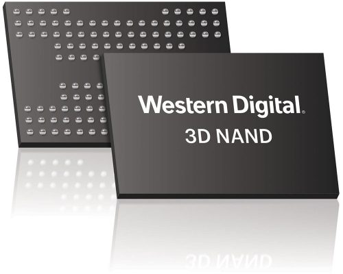
The march of technology never ceases, and Western Digital announces its latest achievement with the creation of 96-layer NAND flash chips. Western Digital’s fourth generation of 3D NAND memory will reach volume production in 2018 and feature TLC, as well as QLC BiCS4 chips.
What is noteworthy is that as recently as last year some analysts theorized that 64-72 layers would be the cap for 3D NAND and that any additional layers weren’t feasible on current process technology. As additional layers are added to a NAND flash chip, additional layer specific TSVs are required to pass through the original layers and link up the entire stack, increasing the fabrication complexity by several factors. Western Digital has evidently surpassed these design issues and is the first to release NAND at whopping 96-layers.
TLC Flash should need no introduction, but QLC may be new to some readers. Quad Layer Cell flash adds a fourth “bit” to the cell creating a whopping 16 voltage states. This increase in storage density has the expected tradeoff of extremely limiting the program-erase cycle endurance of QLC flash down to the 100 – 150 P/E range. As such Western Digital intends to use QLC flash for things like removable USB drives but also special WORM (write once, read many) large capacity datacenter SSDs that act solely as a data repository. In such a usage scenario the low access latency, high read IOPS, and low power operation combined with the additional increase in capacity (or density) that QLC provides would make it a good fit.
Western Digital will be starting off with standard 256Gb dies for 2018 with higher density NAND to follow by 2019. Even with the announcement of BiCS4 today, the storage company has confirmed BiCS5 NAND is naturally deep into development and can be expected around the 2020 timeframe.


