- Qualcomm Launches Snapdragon 4 Gen 2 Mobile Platform
- AMD Launches Ryzen PRO 7000 Series Mobile & Desktop Platform
- Intel Launches Sleek Single-Slot Arc Pro A60 Workstation Graphics Card
- NVIDIA Announces Latest Ada Lovelace Additions: GeForce RTX 4060 Ti & RTX 4060
- Maxon Redshift With AMD Radeon GPU Rendering Support Now Available
Social & RSS Feeds
Latest Videos

Latest News
EVGA GeForce GTS 250 Superclocked
by Rob Williams on March 3, 2009 in Graphics & Displays
The first mid-range offering of NVIDIA’s GeForce 200 series is here, in the form of the GTS 250. As a follow-up to the company’s 9800 GTX+, we already have a good idea of what to expect. But, various improvements aim to make things interesting, such as a redesigned PCB, smaller form-factor, single PCI-E connector, improved temperatures and refreshed pricing.
Page 1 – Introduction
It’s been well over eight months since NVIDIA first launched their GeForce 200 series, and until now, we haven’t seen much from the company in way of mid-range offerings. The closest we’ve come has been with the GTX 260, but at over $200 (much more at launch), it’s still more than some people will want to spend. We can stop waiting for such a thing to arrive though, as the GTS 250 makes its entrance now.
The lead up to this card’s launch has been a little different than most, though, as rumors and speculation of what the card is all about have been soaring through the Internet for the past few weeks. Some of the points made have been valid, some have been false, but if anything’s true, it’s that NVIDIA definitely caught the attention of enthusiasts with this one.
To kick things off, let’s figure out what this card is, and what it isn’t. As rumors have been clear to point out, the GTS 250 utilizes NVIDIA’s G92b core, which is the exact same chip used in their 9800 GTX+. It’s for that reason that some have been quick to throw a quick jab at NVIDIA, since the origin of this GPU was the 65nm G92 – first found in the 8800 GT. Realizing that, it becomes a little easier to understand why some are up in arms.
For the most part, I don’t really blame anyone. I’d like to see a brand-new mid-range core as much as the next guy. But for what it’s worth, NVIDIA isn’t trying to hide anything, and they’ve done well to fully disclose exactly what the GTS 250 is. So, the important thing to note is that they’re not trying to fool anyone into thinking this is something that it’s not, although some may disagree.
Closer Look at NVIDIA’s GeForce GTS 250
What’s going on, then? As pointed out during a press briefing last week, NVIDIA discussed their desire to “simplify” their product line-up. One example used to explain the situation was to take a look at the card that the GTS 250 replaces. At quick glance, a regular consumer may assume that a 9800 GTX+ is much more powerful than, say, a GTX 285, when their performance is in fact on opposite sides of the spectrum. Hence, the need to simplify comes into play.

Throughout the coming year, the company will target their entire current line-up and rename models appropriately, so that when consumers go into a retailer or hop onto an e-tailer, they’ll feel confident in their purchasing decision (although, that would also assume they visited our site first!). Current naming schemes are a real problem, but not only with GPUs. Currently, AMD’s own processors are about to hit the “10K” mark, and Intel hit it not long ago, hence the revised naming scheme for their Core i7 line-up. So, any advances made to simplify product naming schemes is fine by me.
To reiterate, the GTS 250 = 9800 GTX+ in almost all regards, except for some that I’ll talk about now. First, thanks to a board redesign, NVIDIA has shortened the card an entire inch, to settle in at 9″. The GTX 285, by comparison, is 10.5″, so the smaller body of this card will be appreciated by those with a smaller chassis. Also thanks to this board redesign, one power connector was removed, so all you need to power the GTS 250 is a single 6-Pin PCI-E and you’re good to go. Despite these changes though, the TDP is 5W higher on the GTS 250, at 150W.
Another advantage to the GTS 250 is the increase in memory size, to 1GB. The 9800 GTX+ was limited to 512MB, so without even testing, we can be assured that the newer card will fare a bit better in high-resolution gaming (1920×1200+). That said, there will also be a 512MB version of the GTS 250 available, which is ideal for those who want to pair it with their already-existing 9800 GTX+ for SLI. Since the architecture is the same, SLI will work fine as long as the memory densities are the same.
Finally pricing for the GTS 250 1GB is $149, while the GTS 250 512MB will debut at $129. The latter is quite similar to current 9800 GTX+ pricing, although some of those may be had for even less after mail-in rebates. The competition that the GTS 250 goes after is ATI’s Radeon HD 4850 1GB, a card that at recent check, retails for at least $30 more (before mail-in-rebates).
|
Model
|
Core MHz
|
Shader MHz
|
Mem MHz
|
Memory
|
Memory Bus
|
Stream Proc.
|
| GTX 295 |
576
|
1242
|
1000
|
1792MB
|
448-bit
|
480
|
| GTX 285 |
648
|
1476
|
1242
|
1GB
|
512-bit
|
240
|
| GTX 280 |
602
|
1296
|
1107
|
1GB
|
512-bit
|
240
|
| GTX 260/216 |
576
|
1242
|
999
|
896MB
|
448-bit
|
216
|
| GTX 260 |
576
|
1242
|
999
|
896MB
|
448-bit
|
192
|
| GTS 250 |
738
|
1836
|
1100
|
1GB
|
256-bit
|
128
|
| 9800 GX2 |
600
|
1500
|
1000
|
1GB
|
512-bit
|
256
|
| 9800 GTX+ |
738
|
1836
|
1100
|
512MB
|
256-bit
|
128
|
| 9800 GTX |
675
|
1688
|
1100
|
512MB
|
256-bit
|
128
|
| 9800 GT |
600
|
1500
|
900
|
512MB
|
256-bit
|
112
|
| 9600 GT |
650
|
1625
|
900
|
512MB
|
256-bit
|
64
|
| 9600 GSO |
550
|
1375
|
800
|
384MB
|
192-bit
|
96
|
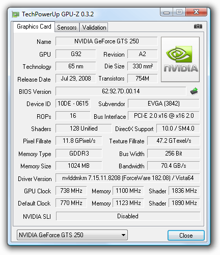
Below, you can see the card’s status report courtesy of the latest version of GPU-Z. Everything here is accurate, aside from the GPU code name and manufacturing process. As already mentioned, this card uses the G92b core, which is built on a 55nm process, not a 65nm one as it appears in the shot. Also seen here are the 128 Shader (or CUDA) processors and 16 ROP units. Overall, the card may be “outdated” by some standards, but it’s still a solid offering for the price, which is the most important thing.
The GTS 250 also features a rather familiar design, one that’s similar for the most part to the GTX 200 cards before it, but smaller. One noticeable difference is that the glossiness of the higher-end cards is lost, replaced with a matte surface (which I actually prefer). Also, despite the card’s budget pricing, you are able to hook three of these guys together for Tri-SLI. It would be an odd route to take (as opposed to purchasing a larger card to begin with), but having the option doesn’t hurt.

Taking a look at the opposite side of the card, we can see the lone PCI-E 6-Pin connector, and also have a good view of the fan. The cooler design is simple in general, but pretty efficient for a stock offering. There’s no doubt that GPU vendors will follow-up to this launch with their own cooler designs, however, which tend to be much better for overclocking and temperatures in general.

You can expect that all of the launch GTS 250’s will look identical, save for the vendor sticker, but similar to the case of our EVGA card here, pre-overclocked models are also sure to be plentiful.
Before we dive into our testing results, one thing I wanted to point out was that while NVIDIA believes the GTS 250’s main competition is ATI’s Radeon HD 4850 1GB, we didn’t have one on hand, to use for the sake of comparison. Also, due to time constraints, we were unable to put the 512MB variant through our most-recent test suite. However, since that’s a 512MB version, the comparison doesn’t matter a great deal at this point. A more appropriate comparison would be with the 9800 GTX+ 512MB, which we do have results for.
So let’s get to it! On the next page, we have our test setup and methodology explained in some depth, and following that, we’ll get right into our Call of Duty: World at War results.

Support our efforts! With ad revenue at an all-time low for written websites, we're relying more than ever on reader support to help us continue putting so much effort into this type of content. You can support us by becoming a Patron, or by using our Amazon shopping affiliate links listed through our articles. Thanks for your support!

Rob Williams
Rob founded Techgage in 2005 to be an 'Advocate of the consumer', focusing on fair reviews and keeping people apprised of news in the tech world. Catering to both enthusiasts and businesses alike; from desktop gaming to professional workstations, and all the supporting software.


