- Qualcomm Launches Snapdragon 4 Gen 2 Mobile Platform
- AMD Launches Ryzen PRO 7000 Series Mobile & Desktop Platform
- Intel Launches Sleek Single-Slot Arc Pro A60 Workstation Graphics Card
- NVIDIA Announces Latest Ada Lovelace Additions: GeForce RTX 4060 Ti & RTX 4060
- Maxon Redshift With AMD Radeon GPU Rendering Support Now Available
AMD’s GTX 760 Killer? MSI Radeon R9 285 Twin Frozr IV Review

It may be a year late, but with its Radeon R9 285, AMD claims that it’s come up with the perfect recipe for taking on NVIDIA’s GeForce GTX 760 – a card that hasn’t seen much of a price drop since its release. Featuring an updated GCN architecture, the R9 285 is an interesting card even outside of its elected battle, so let’s check it out.
Page 1 – Introduction
At this point, it’s no secret that NVIDIA’s next generation GeForce cards are going to be announced soon, and that’s a fact that AMD didn’t want to waste any time capitalizing on. The result of that ambition comes to us in the form of the Radeon R9 285, a card that the company announced during its “30 Years of Graphics & Gaming” event, held two weeks ago.
It’s not uncommon for a GPU vendor to release a new card model in advance of a competitor launch, but this time, things are a little different. You see, the R9 285 isn’t merely a speed-bumped product, or one that’s painfully tweaked to somehow fit inside the normal lineup just because one needs to be there for the sake of quick headlines.
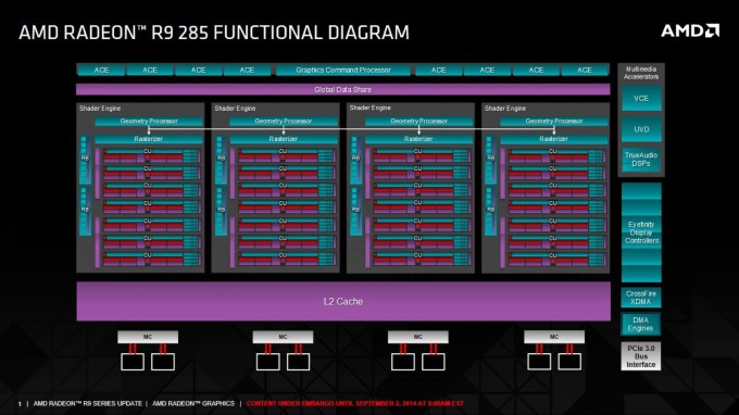
Instead, the R9 285 is the first card to feature the next iteration of AMD’s Graphics Core Next (GCN) architecture. Its core is called “Tonga” (Pro), named after the Kingdom of Tonga, an archipelago in the South Pacific Ocean.
To understand why Tonga, and its future derivatives are important, it’s best to look back to NVIDIA’s launch of Maxwell earlier this year. The first series to be built around Maxwell was GeForce GTX 750, and to say that I was impressed with it (the Ti in particular) would be an understatement. What we had was a ~$150 GPU option that could handle all of today’s games at 1080p resolution and with decent detail levels. As NVIDIA’s GTX 800 (or 900, as it’s rumored to be called) series will also be based around Maxwell, it’s easy to understand why AMD would want to give us a taste of what it has to come.
Let’s take a moment to explain some of what AMD’s promising with its latest GCN architecture. At the forefront, the memory architecture has been vastly improved, promising up to a 40% boost in bandwidth even with a smaller bus width. In a particular example, the R9 285 (256-bit) is shown to peak at just over 40GB/s @ 5500MHz, while the R9 280 (384-bit) @ 5000MHz peaks at just under 30GB/s. That’s without question a very considerable gain.
There are also new 16-bit floating-point and integer instructions that emphasize lower power use in compute and media processing, something that can also dramatically improve transcoding performance when compared to the competition. Another promised boost is with tessellation; AMD says that we could expect a 2~4x improvement in throughput, becoming more effective as the tessellation factor is increased.
Some of the other improvements include parallel instruction processing between the SIMD lanes, an improved compute task scheduler, and a pre-scalar that improves high ratio downscaling quality. Overall, not a lot here that affects gaming specifically, but great enhancements overall.
To gain a better understanding of exactly where the R9 285 fits into AMD’s current lineup, we can make use of this table:
| AMD Radeon Series | Cores | Core MHz | Memory | Mem MHz | Mem Bus | TDP |
| Radeon R9 295X2 | 5632 | 1018 | 8192MB | 5000 | 512-bit | 500W |
| Radeon R9 290X | 2816 | 1000 | 4096MB | 5000 | 512-bit | 250W |
| Radeon R9 290 | 2560 | 947 | 4096MB | 5000 | 512-bit | 250W |
| Radeon R9 280X | 2048 | <1000 | 3072MB | 6000 | 384-bit | 250W |
| Radeon R9 285 | 1792 | <918 | 2048MB | 5500 | 256-bit | 190W |
| Radeon R9 280 | 1792 | <933 | 3072MB | 5000 | 384-bit | 200W |
| Radeon R9 270X | 1280 | <1050 | 2048MB | 5600 | 256-bit | 180W |
| Radeon R9 270 | 1280 | <925 | 2048MB | 5600 | 256-bit | 150W |
| Radeon R9 265 | 1024 | <925 | 2048MB | 5600 | 256-bit | 150W |
| Radeon R7 260X | 896 | <1100 | 2048MB | 6500 | 128-bit | 115W |
| Radeon R7 260 | 768 | <1000 | 1024MB | 6000 | 128-bit | 95W |
| Radeon R7 250X | 640 | <1000 | 1024MB | 4500 | 128-bit | 95W |
| Radeon R7 250 | 384 | <1050 | 1024MB | 4600 | 128-bit | 65W |
When I wrote about the R9 285 not long after its announcement, I put it underneath the R9 280 in this table. The reason for that was simple: The specs told me to. However, paper specs don’t take into consideration architectural enhancements, so clock-for-clock, the R9 285 could be as fast, or a tad faster, than the R9 280.
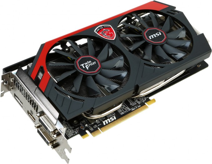
As you’ll see on the results pages, the MSI Radeon R9 285 Twin Frozr IV edition we were supplied with is in fact a bit faster than the R9 280 – at least, against Sapphire’s Dual-X version of the R9 280. For comparison’s sake, the reference R9 280 peaks at 933MHz, whereas Sapphire’s version capped at 950MHz. The reference R9 285, by contrast, peaks at 918MHz, while our MSI sample bumps that to 973MHz.
Where the biggest difference lays – not counting the architecture change, of course – is with the total memory. The R9 280 has 3GB of GDDR5 on tap, while the R9 285 has to settle with 2GB. That’s something that our results will prove won’t matter much, or at all, for most people.
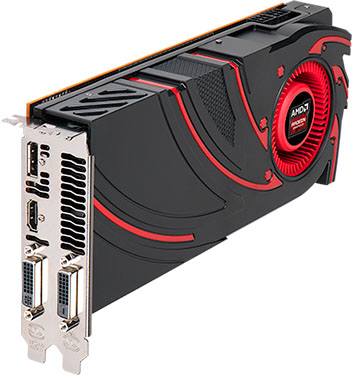
The picture of the MSI card above was thieved from the company’s website, and it’s actually of its R9 270X Twin Frozr IV. The cards do look the exact same, however, with both its cooler and ports (2x DVI, 1x HDMI, and 1x DisplayPort). As I’m currently inundated with content, I took the easy way out this time with regards to the photography.
With that all said, let’s get a move on and pit the R9 285 against all of the cards that surround it in AMD’s and NVIDIA’s respective lineups.
Support our efforts! With ad revenue at an all-time low for written websites, we're relying more than ever on reader support to help us continue putting so much effort into this type of content. You can support us by becoming a Patron, or by using our Amazon shopping affiliate links listed through our articles. Thanks for your support!


