- Qualcomm Launches Snapdragon 4 Gen 2 Mobile Platform
- AMD Launches Ryzen PRO 7000 Series Mobile & Desktop Platform
- Intel Launches Sleek Single-Slot Arc Pro A60 Workstation Graphics Card
- NVIDIA Announces Latest Ada Lovelace Additions: GeForce RTX 4060 Ti & RTX 4060
- Maxon Redshift With AMD Radeon GPU Rendering Support Now Available
Is NVIDIA’s GF100 Broken and Unfixable?
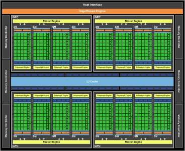
If there’s ever been a huge amount of doubt surrounding an upcoming product, NVIDIA would have to take gold with the help of its Fermi architecture. There’s been a couple foiled starts, and reason to believe that GF100 might have some issues that are proving very difficult for the Santa Clara company to fix. Charlie Demerjian, in his usual way, explains why he believes Fermi is not going to happen properly anytime soon.
To preface anything I’ll say here, I consider Charlie to be a friend, and that anything he writes about generally has some grain of truth to it, even if he isn’t spot on. He’s incredibly knowledgable in anything he writes about, but nothing can be considered fact until it’s just that… an absolute hard fact. With Fermi, I’m not sure what to think, especially after reading his amazingly-thorough rant.
The first and most important issue Charlie raises is the fact that Fermi is unbuildable where the law of reason exists. For a company like NVIDIA to make money, there has to be a good return-of-investment on the products it’s going to send through R&D. According to Charlie’s look at things, because Fermi is built on a monolithic die, and has such a poor yield rate (which is rumored to be as low as 2%), there’s no realistic hope of earning money on the architecture.
Last week, I linked to an article that Anand wrote that took a look at the life of RV870, and in it, he mentions that one hurdle AMD had to overcome was the instabilities of the interconnects. One method to fix this was to double the number of vias, and according to Charlie, that’s something that NVIDIA needs to do as well. But, that won’t fix the yields. When ATI tested the 40nm TSMC waters with RV740, in order to avoid diving right in with the big boys, it was able to figure out what would need to be fixed in order to avoid major issues. NVIDIA, according to Charlie, did little homework, and decided to go the “bull in a China shop” route.
Yet another potential major issue with Fermi, is that if certain things are fixed, what might result is an even higher power consumption. The high-end chip as it stands today is rumored to settle in at around 280W TDP, and given that cards at over 300W can’t be certified for PCI-E use, there could be a real issue. Charlie believes that while we should be seeing some Fermi cards in the near-future, the samples will be limited, and will be used for little more than a PR stunt.
I’m not quite as familiar with chip manufacturing as Charlie is, nor discuss Fermi with NVIDIA’s engineers or others, so I’m not sure what to think. It’s clear that NVIDIA has had issues with Fermi from the get-go, but after what we saw during the company’s editor’s day last month, it’s hard to say that the company is still battling with the architecture and 40nm yields without actually being in the company. I certainly hope that we’ll see a natural Fermi launch soon, not only because it would be nice to see some sweet competition to ATI’s HD 5000-series of cards, but because NVIDIA desperately needs something to pick it up out of its funk.
Edit: It appears NVIDIA announced via its Twitter feed (*sigh*) that the launch date will be March 26, for both the GTX 470 and GTX 480. The cards will also be shown off at PAX East!

The two real fixes, doubling the vias and redesigned circuits to minimize the impact of transistor variances both require a full re-layout. Both also cost time and die area. The time is at least six months from tapeout, if you recall. Fermi taped out in late July and was only slated for small numbers at retail in late November, a very unrealistic goal. A B1 spin of the chip would be at least Q3 of 2010 if it tapes out today, and it won’t have a useful life before it is supplanted by the next generation of 28nm chips.


