- Qualcomm Launches Snapdragon 4 Gen 2 Mobile Platform
- AMD Launches Ryzen PRO 7000 Series Mobile & Desktop Platform
- Intel Launches Sleek Single-Slot Arc Pro A60 Workstation Graphics Card
- NVIDIA Announces Latest Ada Lovelace Additions: GeForce RTX 4060 Ti & RTX 4060
- Maxon Redshift With AMD Radeon GPU Rendering Support Now Available
Introducing AMD’s Latest Generation GPU Architecture: Polaris

After a long delay, AMD begins to divulge information on its new 4th generation GCN GPU architecture: Polaris. With it comes improvements to data handling, power efficiency, new hardware features, and a design overhaul for smaller manufacture processes; 14-16nm FinFET.
Well, it looks like we’re going to be in for an interesting year. Details and rumors about AMD’s Arctic Islands generation of GPUs have been rather limited, but slowly, information has been coming forward. The latest of which is the name and high-level overview of the new architecture that will be at the heart of AMD’s latest chips.
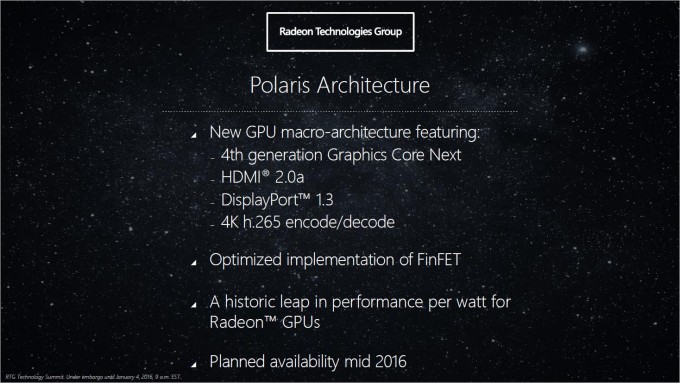
Polaris is the new codename for the architecture that will be forming the core of the latest generation of GPUs from AMD. More than that, we have some details and specs that cover the transition from the now very aged 28nm process, to the new 16nm FinFET based manufacture process.
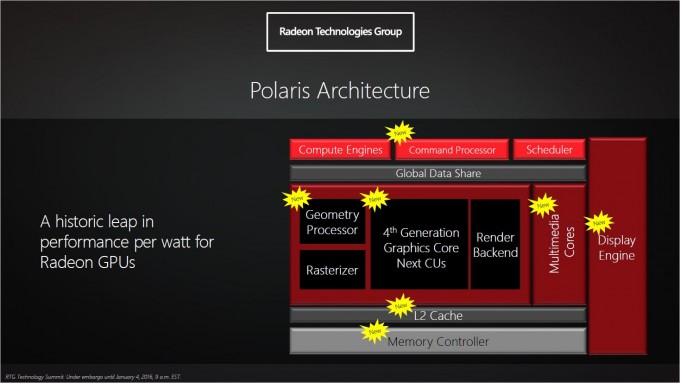
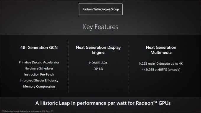
4th Generation GCN
While Fury introduced HBM (stacked die memory), the architecture was still the same GCN 1.2 (third generation) as used in the 200 and 300 series GPUs. With Arctic Islands, AMD is in a somewhat odd position of introducing both a new manufacturer process and a new architecture at the same time. Normally, the two are staggered, allowing for design maturity to be focused on one or the other.
The high level overview of the architecture focuses a lot more on efficiency more than anything, with a couple extra hardware features. At its core, there is a new geometry shader, ideally used for physics calculations. There are larger buffers, including a new L2 cache system. Improved shader efficiency and memory compression, which is also tied to better data pre-fetch. This all neatly ties in with AMD’s bigger push for its GPUOpen initiative; expanding the capabilities of the GPU when it comes to workstation and general computation.
We will see HDMI 2.0a rolled out finally, along with DP 1.3. This has two main effects. The first, and probably most important, is removing the bottleneck on the GPU when it comes to 4K displays being limited to 30Hz for HDMI, and 60Hz for DisplayPort. What’s also interesting is that AMD has figured out a method to support FreeSync over HDMI 1.4 as well (of course, a compatible monitor is still required).
On the multimedia side, it’s all about h.265, or HEVC if you prefer – the 4K video stream codec. On the decoder side, there is hardware support for the main10 profile up to 4K, meaning 10-bit color support. On the encoder, 60 FPS at 4K is supported too.
FinFET
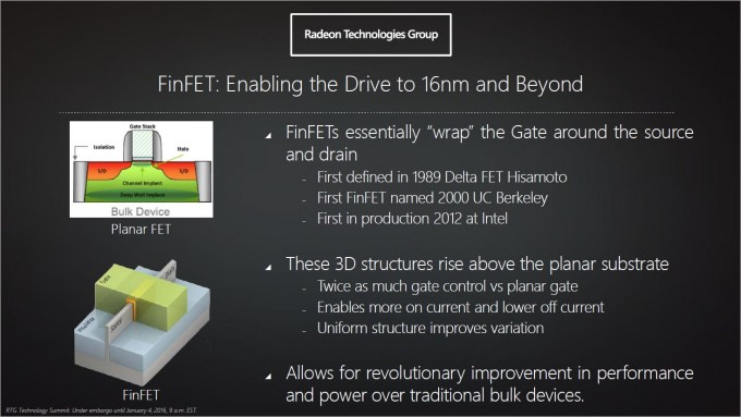
Arguably, the biggest change overall will be the switch in manufacture process from 28nm down to 16nm and 14nm with FinFET – this is a huge reduction in process size. AMD had experimented with reductions in process size before, but was largely unimpressed with the results. In fact, NVIDIA skipped the 20nm process as well, even with its latest GPUs.
AMD indicated through the press release that the main contributing issue was transistor leakage. As the manufacture process gets smaller and smaller, so too does the gap in the insulative layers; allowing current to flow through it or escape, leading to excessive power consumption and/or data corruption.
Intel had similar issues a few years ago, which is when it introduced its own FinFETs into the equation back in 2012. FinFETs can be best described as 3D switches, with the gate extending over a larger area, providing more surface contact with the source and drain, enabling better control over switching. Less power is needed, it becomes more sensitive, and can enable more power to flow through the switch if need be.
A lot of the delay with the switch to FinFET comes from the manufacturer, TSMC, which is used by both NVIDIA and AMD for their respective GPU manufacturing. The same tired 28nm process has been in used now for four years; three generations of GPUs. While TSMC does have a 20nm process available, it’s mainly used for SoC based products, rather than monolithic and complex chips such as GPUs.
It’s All About Power
While improvements to the architecture are most welcome, AMD is banking a lot more on FinFET, and the massive power savings that come with it. In fact, when you flick through the slides in the press release, you’ll find that half of them talk about the improved efficiency that comes as a result of FinFET and corresponding die shrink.
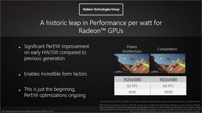
AMD included an in-house benchmark, showing the improvement in power over the ‘competition’. Playing the latest Star Wars game, Battlefront, AMD put its latest test system against an NVIDIA GTX 950 (desktop, we presume). No details about the name and model of the Polaris card used, but both were playing Battlefront on medium settings at 1080p, 60 FPS, with the GTX 950 drawing 140 Watts, while the AMD Polaris card only using 86 Watts.
Now, some amount of context is required here as well. The typical power management improvement we expect to see from switching from the now aging 28nm process down to 16nm, is about 60%. The comparison of cards above show a 61% drop in power. Now, we know from previous cards that AMD has used slightly more power than NVIDIA , so the 60% power drop shows more than just the FinFET at work, as the architecture has been improved too. More importantly, this is on a pre-release card with limited optimizations.
From what we are told, AMD expects to see high double-digit performance gains across the board with all its latest generation GPUs. When the cards are finally released, we’ll be putting these claims to the test.
Speaking of release, things are still largely up in the air. What we know is that we expect to see mobile based products around summer time (mid 2016 is as specific as it gets), so presumable we’ll see the first iteration of desktop parts some time in the spring.
This release date is approximately when we expect to see NVIDIA’s latest iteration of chips (Pascal for those keeping track), that also happen to use the same 16nm process from TSMC. It looks like we’ll finally see an interesting mix of launch technologies this year, something long overdue.
Support our efforts! With ad revenue at an all-time low for written websites, we're relying more than ever on reader support to help us continue putting so much effort into this type of content. You can support us by becoming a Patron, or by using our Amazon shopping affiliate links listed through our articles. Thanks for your support!


