- Qualcomm Launches Snapdragon 4 Gen 2 Mobile Platform
- AMD Launches Ryzen PRO 7000 Series Mobile & Desktop Platform
- Intel Launches Sleek Single-Slot Arc Pro A60 Workstation Graphics Card
- NVIDIA Announces Latest Ada Lovelace Additions: GeForce RTX 4060 Ti & RTX 4060
- Maxon Redshift With AMD Radeon GPU Rendering Support Now Available
NVIDIA GTC 2020: Ampere A100, Drive, Jarvis, Merlin & A Whole Lot Of Mellanox

NVIDIA has released all of its GTC announcements en masse today, and as expected, there is a ton of information to pore over. We’re taking a look at most of what was announced, including, of course, a look at the company’s new top-end data center GPU: the Ampere-based A100.
As planned, NVIDIA released its belated GTC 2020 keynote online earlier, and it’s a reminder that we’re living in really interesting times. Rather than a live broadcast, everything posted has been prerecorded, straight from Jensen’s home (specifically: the kitchen) in California.
Jensen starts his keynote off by thanking everyone involved in the fight against COVID-19, from doctors to truck drivers. He goes on to mention that NVIDIA has been working heavily with scientists around the world to enhance containment, mitigation, treatment, and ultimately, tracking and monitoring. He boasts that with NVIDIA tech, Oxford was able to sequence the virus genome in a meager seven hours.
And that right there is why this GTC comes at a good time. If someone didn’t understand the importance of computing in the fight against diseases, chances are good that COVID-19 has opened their eyes. When the pandemic creeped up, unparalleled efforts around the world instantly focused on battling this virus. NVIDIA has long talked about using its GPUs for this very purpose, so it has reason to gloat here.
NVIDIA’s Ampere-based A100 & DGX A100
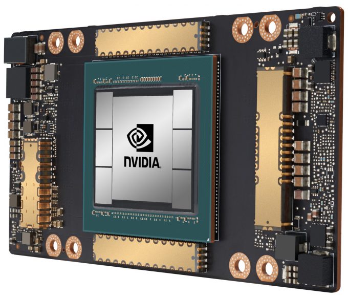
Without wasting time, let’s get right to what most people reading this will be curious about: NVIDIA’s new graphics hardware. As expected, the latest flagship architecture is Ampere, and following tradition, it’s led to an “A100” GPU:
Like the Pascal-based P100 and Volta-based V100 before it, the Ampere-based A100 is designed from the ground up for the data center. The A100 becomes NVIDIA’s first 7nm GPU, built at TSMC, and it utilizes third-gen Tensor cores, NVLink, and NVSwitch.
| NVIDIA P100 | NVIDIA V100 | NVIDIA A100 | |
| Transistors | 15.3 billion | 21.1 billion | 54 billion |
| Die Size | 610 mm2 | 815 mm2 | 826 mm2 |
| SMs | 56 | 80 | 108 |
| Tensor Cores | N/A | 672 | 432 |
| Peak Tensor TFLOPS | N/A | 125 | 312 |
| FP64 CUDA Cores | 1,792 | 2,560 | 3,456 |
| FP64 Performance | 5.3 TFLOPS | 7.8 TFLOPS | 9.7 TFLOPS |
| FP32 CUDA Cores | 3,584 | 5,120 | 6,912 |
| FP32 Performance | 10.6 TFLOPS | 15.7 TFLOPS | 19.5 TFLOPS |
| Memory Density | 16GB HBM2 | 16GB HBM2 | 40GB HBM2 |
| Memory Bandwidth | 732 GB/s | 900 GB/s | 1,555 GB/s |
NVIDIA has a few technologies that have gone into the A100 worth talking about, right down to the die. With TSMC, NVIDIA has built a design around CoWoS (chip-on-wafer-on-substrate) packaging, which puts the memory and GPU on the same substrate, delivering the fastest possible access between them. With its improvements, the effective memory bandwidth jumps from 900 GB/s on the V100 to roughly 1.6 TB/s on the A100.
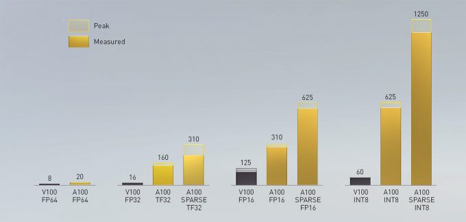
As mentioned, this design also brings forth the third-generation of Tensor cores, which introduces TF32 (TensorFloat32). With it, any FP32 code imported can be processed as FP16, all without code changes. In an example between V100 and A100, the new Ampere card processed its matrix operations six times quicker.
Also new is sparsity, a feature that can effectively boost performance by 2x. It works by taking an original dense network, zeroing out all of the small weights, and then retrain with the same data structure and pipeline. As the above chart shows, it’s not just one type of computation that benefits from this sparsity feature, but many.
The ultimate top-end performance metric for the A100 is 1.25 POPS – or 1,248 TOPS, representing INT4 (before sparsity), with INT8 half that. You can just imagine how much performance would be available to those equipped with a new A100 compute platform, which comes complete with 8 of the new top-end GPU.
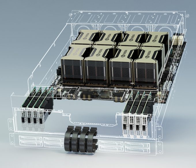
According to Jensen, this A100 platform board weighs 50lbs, sports 600GB/s NVLink connections, six NVSwitches, one million drill holes, over 1 kilometre of traces, and over 30,000 individual components. With eight of these A100 GPUs, you’d have a total of 320GB of 1.6 TB/s memory, and 55,296 CUDA cores.
“MIG”, or “Multi-instance GPU”, is another technology introduced with the A100. With it, one GPU can be split up into (up to) seven separate interfaces, allowing multiple users to take advantage of the same hardware to process their workloads. This is useful for cloud instances where such partitioning could end up reducing the cost-per-user.
A MIG demo consisted of inference on a collection of bird sounds, working to detect which chirp came from which type of bird, with super high accuracy. While that operation on a full A100 is incredibly fast, using MIG to separate one card into seven instances of a GPU will largely deliver the overall inference performance of a V100 to just one of the MIGs in this particular test. With V100, the example showed about 80 queries per second, while with a full A100, that jumped to over 500.
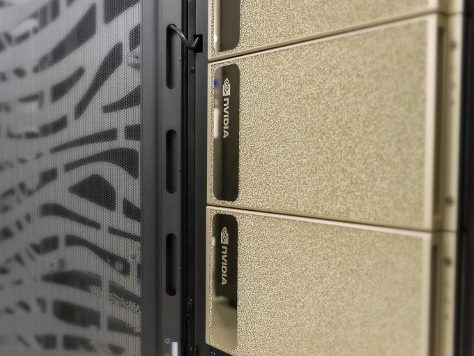
Naturally, that big platform board pictured above needs to be put into an actual usable platform, so that’s going to become the new DGX A100, offering 5 PFLOPS of total AI performance.
In addition to the six NVSwitches, the DGX A100 includes nine Mellanox ConnectX-6 HDR 200Gbps NICs and in-network acceleration engines, 15TB of internal PCIe 4.0 SSDs, and dual processors. Those processors happen to be 64-core AMD EPYC 7742, offering a total of 256 threads to the system. Because those CPUs also need to breathe, there’s a healthy 1TB of system RAM. All of this can be yours for $199,999 – and remember: “The more you buy, the more you save”.
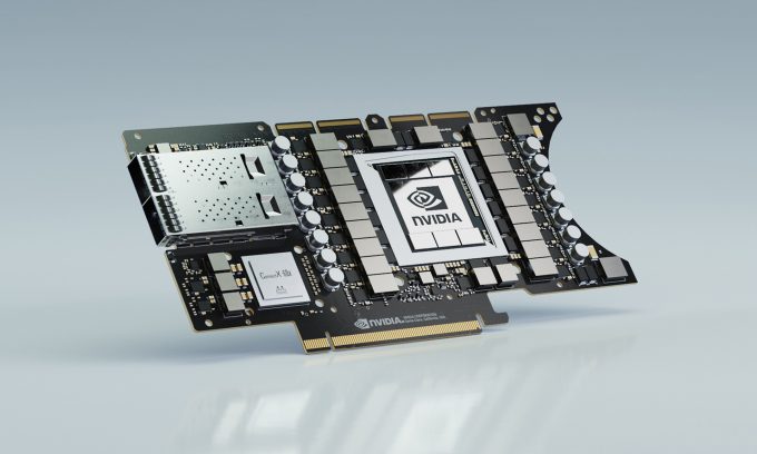
Here’s the Ampere A100 GPU once it’s slapped onto an EGX (Edge Computing) card, which has also been announced today:
This isn’t your average GPU, to say the least. The chip seen to the left is Mellanox’s ConnectX-6 DX, which offers dual 100Gbps Ethernet or InfiniBand connections. If it wasn’t clear to you why NVIDIA acquired Mellanox by now, a picture like that should make it obvious. Installing this into a server turns it into a hyper-converged AI powerhouse, or as Jensen puts it, “an entire cloud data center in one box”.
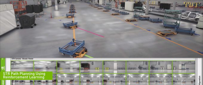
One example of this A100 card’s use is in robotics, as the processing horsepower is unparalleled, as is its networking capabilities. BMW has already gotten on board with NVIDIA’s Isaac platform, with plans to “build the factory of the future”. That at the very least means there will be many robots making the rounds throughout the process of building a Bimmer. Considering the amount of models and individual options that a carmarker like BMW offers, it’s easy to understand why the help of robots, and increased automation in general, could prove to be a boon for this kind of environment.
Mellanox, Mellanox, Mellanox
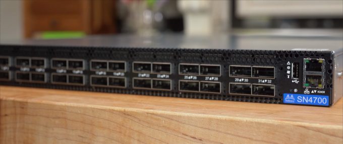
The very first product Jensen showed off in NVIDIA’s series of videos wasn’t actually the Ampere-based A100 that everyone has been most hyped over, but instead a new Mellanox Spectrum 4000-series Ethernet switch. Each of the ports on this switch can scale up to 400Gbps, which is rather incredible when you consider most home users are still stuck on 1Gbps, or 10Gbps at the high-end.
With this switch, data buffering is used to meter the bandwidth across the entire unit, so that each port gets their fair share of resources, while virtualization can be used to spread VX LAN throughout an environment. A third feature talked about is “WJH” (What Just Happened), which uses advanced telemetry to better diagnose networking problems.
Inside of this beastly switch is a Mellanox BlueField-2 programmable NIC, which is an example of a third processor that has officially become integral to moving massive amounts of data around. For general compute, there’s the CPU, while for accelerated compute, there’s the GPU. For network? We have the DPU, or “Data Processing Unit”, responsible for moving data as quickly as possible throughout a data center.
DLSS & Ray Tracing
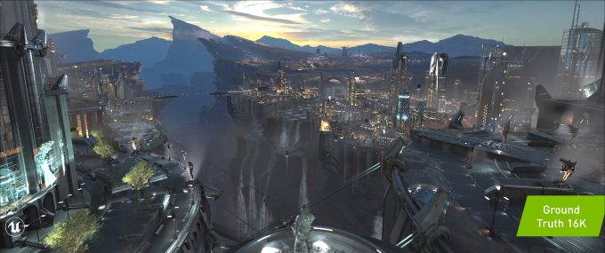
Jensen talked about the progress its DLSS (deep-learning super-sampling) technology has made since its unveiling alongside the RTX launch in late 2018. Ultimately, resolution has vastly improved, enabling a 1080p DLSS render to look even sharper than native 1080p – or so is the claim (that we need to test soon). Ray tracing is also brought up, as Minecraft has been updated to support both technologies in unison, allowing players to roam an environment with completely realistic lighting. Just be warned: you’re going to want a powerful GPU.
Speaking of powerful GPU, a single Quadro RTX 8000 powered a Marbles RTX demo that looked stunning. A player takes control of different marbles, rolling them around the environment to ultimately reach an end goal. Marble Madness of old definitely comes to mind, and if we had have seen these graphics back then, we probably would have literally lost our minds.
The important thing to note with this demo is that absolutely everything is in real-time. The lighting isn’t baked-in, but instead driven through ray tracing, and the end result is hugely convincing. The physics are likewise realistic, and all we could really think during the demo is that we’d very much like to try it.
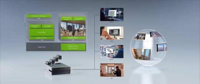
Tying into the ray tracing aspect a little bit, NVIDIA also announced Omniverse today, which is a full platform for collaboration in creative or industrial design. The base of Omniverse consists of an RTX server, which can use a virtual server to dole out resources to everyone according to needs. Because collaboration is the name of the game here, users tackling different projects can all work on the same server, and share assets and content easily. NVIDIA calls these environments “portals”, a shared world that should speed up development time (and perhaps improve sanity?)
NVIDIA so far has added Adobe, Autodesk, Pixar, Rhinoceros, SideFX, Trimble, Unreal Engine, and Unity to its Omniverse partners list, so the support from the get-go is quite strong here.
GPU-accelerated Datasets with Spark
The funny thing about technology is that what seems mind-blowing today may not seem so mind-blowing in just a few years. When it was released, the Pascal-powered Tesla P100 was a screamer of a GPU, and really, it still is. But with the introduction of Tensor cores, you really need to go current-gen if you want the best possible performance, and not to mention the best efficiency.
When it comes to big data, bottlenecks have changed a little bit over the years. Today, the amount of data that has to be processed in large projects is simply incredible, and NVIDIA believes that today’s biggest bottleneck in server crunching is the CPU. When a CPU has tens of megabytes of cache whereas a GPU can have tens of gigabytes, workloads that can go on the GPU probably should. While any on-die cache is going to be quicker than external memory, CPU-bound memory will not be as fast as NVIDIA’s on-substrate HBM2.
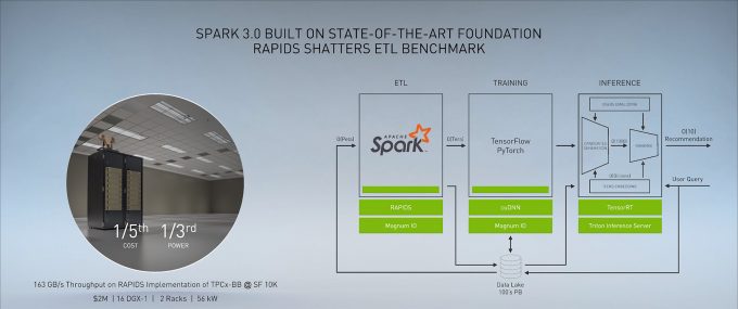
The upcoming release of the hugely popular Apache Spark (3.0) is going to see to it that GPUs start working on more unique workloads, as it’s going to become GPU-aware, and can use its scheduler to smartly partition work across the entire system. Part of this is made possible by another team effort with Mellanox: GPU direct storage. With it, the IO is accelerated, vastly reducing bottlenecks in multi-node systems.
Hardware is just one part of this whole equation, but software is just as important. NVIDIA’s updated its RAPIDS libraries to work with Spark 3.0 to ensure ultimate efficiency, as it’s able to intercept queries and direct them accordingly.
With all of this put into place, NVIDIA says that you can deliver better performance with RAPIDS at 1/5th the cost, and 1/3rd the power, versus a typical competitor, and we all know what that means. “The more you buy, the more you save.” Databricks is a use-case mentioned, as it was built entirely around Spark to manage massive datasets, and as a service that spins up a literal million virtual machines a day, it’s a good nod to NVIDIA to see it backing these efforts. Other platforms that are joining in on this bandwagon include Amazon SageMaker, Azure Machine Learning, and Google’s Cloud AI and Cloud Dataproc.
NVIDIA Merlin Recommender Acceleration
Something we bump into pretty much every day are “recommenders”. If you’re a Spotify user, you’ll see suggested playlists and songs. On Netflix, you’ll be suggested shows similar to what you and other users with similar interests are likely to enjoy. In other uses, recommenders could be used for healthcare therapy suggestions, and for automation throughout a sales process.
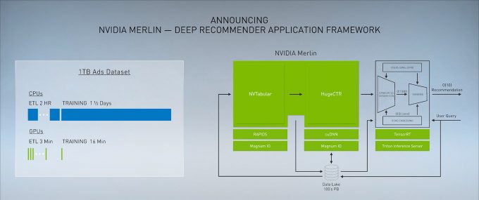
The problem with recommenders is that they are extremely complex, and that’s something NVIDIA naturally wants to help with. So, it’s created Merlin, a complete framework that allows people to easily create dataframes that can process tens or hundreds of terabytes of data, with all partitioning and scaling done automatically.
It’s being touted that you can write just a few lines of code with NVTabular to get up and running quickly, while the rest of the pipeline will involve HugeCTR for the acceleration of learning ranking systems. All of this is built on top of RAPIDS and cuDNN, and as the graphic above suggests, what it takes a CPU to do in one-and-a-half days will only take a top-end GPU sixteen minutes to pull off.
The sixteen minutes used to train here was only with 1TB of data, so if the delta between thirty-six hours and sixteen minutes doesn’t seem impressive enough, consider the dramatic differences if many or hundreds of terabytes are needing to be dealt with. NVIDIA is launching Merlin with petabyte datasets in mind, so it seems like it’s ready for anything.
NVIDIA Jarvis Conversational AI
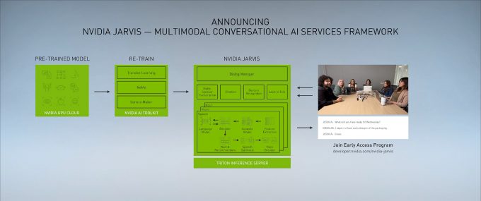
We’ve heard about NVIDIA’s Jarvis before, but today, the company unveils some major updates to its usefulness. Jarvis is one of NVIDIA’s products that relies hugely on its TensorRT libraries, which have just reached the seventh generation. TensorRT now enables support for RNNs, and offers automatic mixed-precision processing between FP32/FP16/INT8.
Jensen says that conversational AI is one of the most intensive uses of inference, and that becomes especially true when what’s trying to be achieved is true interaction. You can talk to Siri and get an answer back quickly, but NVIDIA wants you to be able to talk face-to-face with an avatar, and all responses be quick, and realistic.
Jarvis uses a series of technologies in its pipeline, including automatic speech recognition for activating instantly, natural language understanding for interpretation of what’s being said, text-to-speech speech recognition, as well as audio-to-face, which produces the resulting output. To have all of this done in an instantaneous manner is hugely challenging.
A demo was shown of a conversational AI avatar named Misty, an interactive chat bot. Jensen asks some basic questions, such as the weather, but ultimately highlights its ability to contextually understand what you’re talking about. “Do I need an umbrella?” will lead to weather feedback from where you are located. When asked about the coldest current place on earth (Yakutsk, Russia), Misty turned ice cold and dropped to the floor, adding a lot of life to a mere bot.
Jensen said that all of the Jarvis models found in its NGC (NVIDIA GPU Cloud) represents several hundreds of thousands of hours of DGX training, so to call it comprehensive would be an understatement. It will, of course, only get even better as time goes on. If you had one DGX, which includes 8 top-end NVIDIA graphics cards, it’d take well over ten years to train models like these.
Ampere Hits NVIDIA Drive
NVIDIA’s latest computing architecture generally finds its way to its Drive platform sooner than later, but there has been no time at all wasted here. NVIDIA says that Ampere can power devices as small as 10 TOPS and 5W for assisted driving, and scale up as high as 2,000 TOPS and 800W for fully autonomous robotaxis.
You can see a cool example of the latest iteration of NVIDIA Drive at the 2m 20s mark in the video above. All of NVIDIA’s employees who have been working on this technology have been safe at home, with much of the work being done in VR. In a completely virtual environment, they are able to use Drive to autonomously drive to work, and not have to deal with unsightly billboards.
Final Thoughts (For Now)
NVIDIA’s GTC sure didn’t go according to its original plan, but it’s been no less exciting hearing about all of the news a couple of months late. The Ampere A100 is close to the GPU we would have expected, although some rumors got quite a bit wrong. What we ultimately see is, compared to the V100, a 24% boost to single- and double-precision performance, and a massive jump in AI performance. Not to mention a whack of boosts to other metrics, like memory bandwidth.
These latest-gen GPUs are built from the ground up for data center and AI use, and it shows. The fact that NVIDIA is putting Mellanox chipsets directly on its EGX card shows just how serious it is about the edge, and also bandwidth. With the DGX A100, the level of performance delivered is simply astonishing, and with sparsity, which can boost inference performance by a factor of two, it could become doubly as impressive.
The Mellanox deal didn’t close long ago, but NVIDIA’s made its reasons for acquiring the company clear, and we’re already seeing just how tightly integrated into NVIDIA the company is becoming. Speaking of being integrated, Omniverse is also a notable project, allowing full teams to work together from the same hardware, with a huge focus on collaboration.
Technologies like the Jarvis voice conversational AI and the Merlin recommender platforms are also notable in their own right, and of course, both will be accelerated better with Ampere than anything to come before it.
The focus of Ampere so far has been entirely on the data center, and based on its major focus on that very environment, it’s not an architecture that would translate easily to gaming. You may recall that Volta was largely expected to be featured in a GeForce at some point, but instead, the next step was Turing, which introduced ray tracing cores to sit alongside the Tensors that were shared by the Volta design.
If you’re a gamer, it might be a bummer that nothing specific to you was revealed today, but the data center is truly the biggest focus of NVIDIA’s GPU Technology Conference. We have no clue when NVIDIA is planning to unveil its next GeForce or Quadro series, and since we’re poor guessers, we will let you folks speculate on when you think they’ll arrive.
Support our efforts! With ad revenue at an all-time low for written websites, we're relying more than ever on reader support to help us continue putting so much effort into this type of content. You can support us by becoming a Patron, or by using our Amazon shopping affiliate links listed through our articles. Thanks for your support!


